
Project
An FPGA IoT gateway with a custom AES core
From a VHDL AES-128 core to live sensor readings: a Nexys A7 gateway with bare-metal C firmware, Ethernet telemetry, and a Python controller.
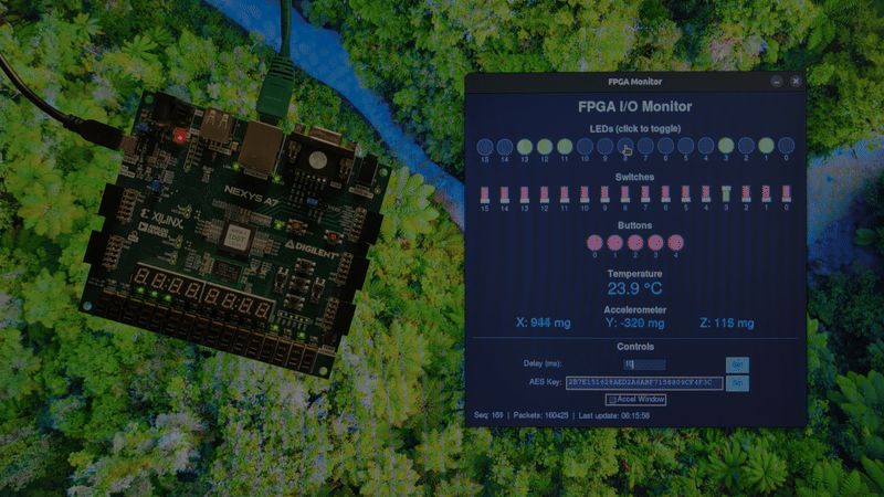
Move the board and the acceleration readings change. Press a button and its indicator lights up on the computer. Click an LED in the controller and the physical LED toggles. Between the board and the screen, each sensor update passes through an AES-128 core I wrote in VHDL.
I built this gateway in January 2026 for Sistemas Integrados para Aplicações Embutidas at the University of Aveiro. I implemented the encryption core, its AXI interface, the bare-metal firmware, and the Python controller. The hardware target is a Nexys A7-100T, with an Artix-7 FPGA and a MicroBlaze RISC-V soft processor running at 100 MHz.
The processor has company
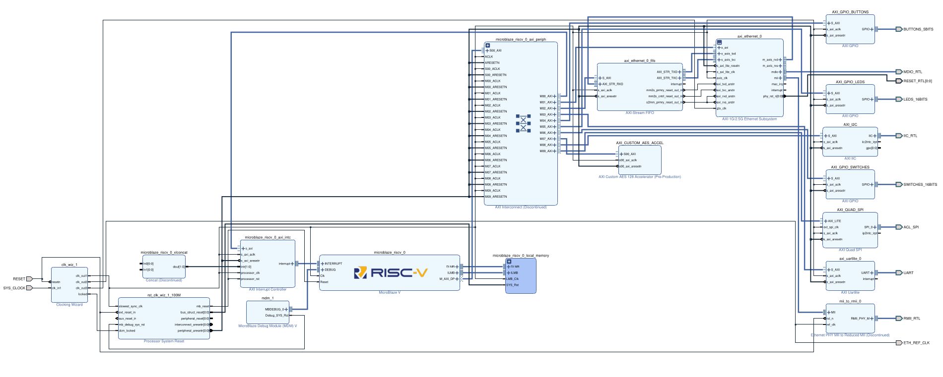
The processor reads sensors, assembles packets, and handles commands. AES runs in a separate hardware peripheral, connected over AXI alongside the GPIO, I²C, SPI, UART, and Ethernet interfaces. From the firmware’s point of view, encrypting a block means writing and reading memory-mapped registers.
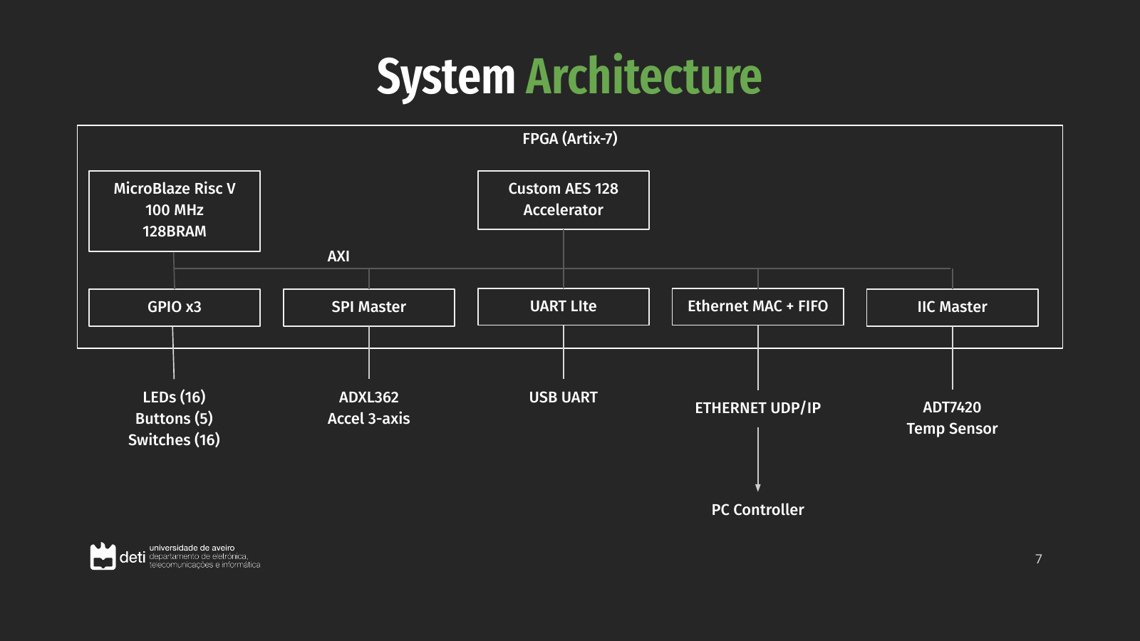
The board’s temperature sensor and accelerometer give the system something observable to transmit. The return path makes it easier to check the whole chain: a command from the desktop changes an LED, then the next sensor packet reports that changed state.
One round circuit, used ten times
The AES core accepts a 128-bit key and one 128-bit plaintext block. Internally, the state is a four-by-four matrix of bytes. The VHDL separates SubBytes, ShiftRows, MixColumns, AddRoundKey, and key expansion into modules, so each transformation can be checked on its own.
The round circuit is reused across clock cycles. The state machine first XORs the plaintext with the initial key, executes nine regular rounds, then a final round that skips MixColumns. Key expansion produces the next round key alongside the data path, using the previous key and the round constant.
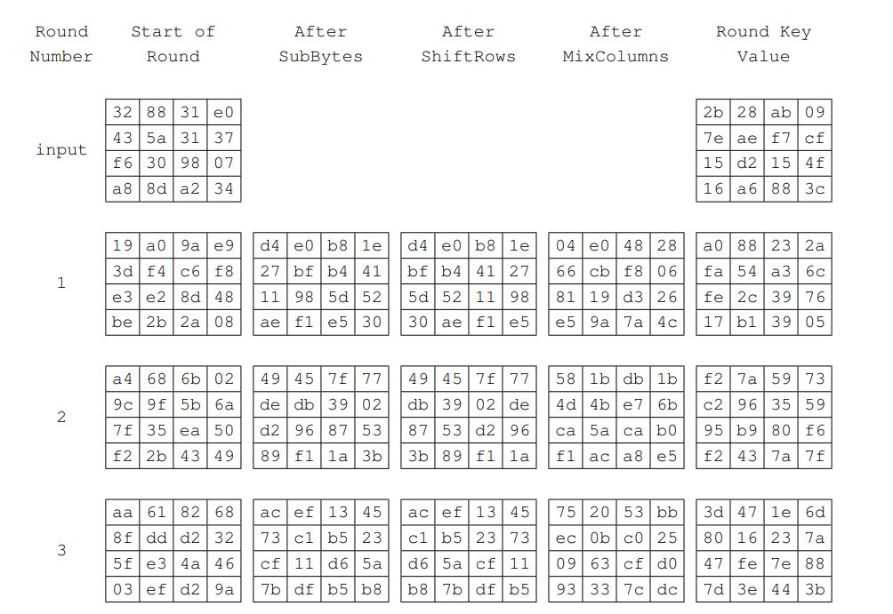
MixColumns looks like matrix multiplication, but its byte arithmetic becomes shifts and XORs. For example, this is the working part of gf_mult_by2.vhd, with comments omitted:
shifted <= byte_in(6 DOWNTO 0) & '0';
mask <= x"1B" WHEN byte_in(7) = '1' ELSE
    x"00";
byte_out <= shifted XOR mask;
The conditional 0x1B applies the reduction required by the AES finite field. Multiplication by three then uses that result XORed with the original byte. In aes_round.vhd, a multiplexer selects the ShiftRows output directly on the last round, bypassing MixColumns before the round-key addition.
Checking the result before adding Ethernet
The testbenches cover the individual transformations and the assembled core. The full-core testbench checks four known answers, including NIST examples and an all-zero key and plaintext. A mismatch raises an assertion failure; the suite runs with make run-all in CoreAes128.
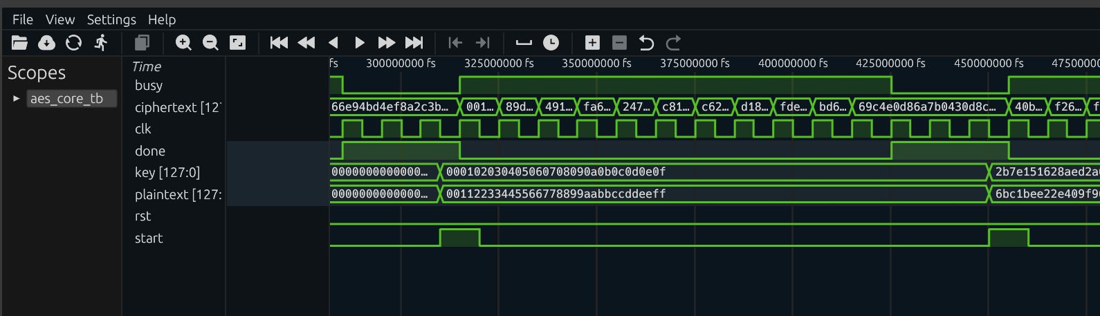
The handshake is deliberately small: start, busy, and done. A rising edge on start begins a block. The controller keeps busy asserted while it works and raises done after the final result. Processing takes roughly twelve clock cycles, including the control steps; that is the core’s latency, rather than the duration of the C call or a network update.
Turning the core into an AXI peripheral
I packaged the core as an AXI4-Lite IP block in Vivado. Its 32-bit registers split each 128-bit value into four words:
| Offset | Registers | Access | Contents |
|---|---|---|---|
0x00 | CTRL | Read/write | Bit 0 drives start |
0x04 | STATUS | Read | Bit 0: done; bit 1: busy |
0x08–0x14 | KEY0–KEY3 | Read/write | Key, most significant word first |
0x18–0x24 | PT0–PT3 | Read/write | Plaintext, most significant word first |
0x28–0x34 | CT0–CT3 | Read | Ciphertext, most significant word first |
The wrapper concatenates the four key registers and the four plaintext registers into the core’s inputs. It also inverts AXI’s active-low reset for the AES core’s active-high reset.
The C driver clears start, writes the key and plaintext, sets start, polls STATUS.done, and reads four ciphertext words. Clearing start again prepares the next rising edge. Polling is enough for this sensor application, where the default interval between packets is 500 milliseconds.
Byte order needs to stay consistent through the registers, the packet, and Python’s decoder. This helper makes the register representation explicit:
static u32 pack_bytes(const u8 *b) {
    return ((u32)b[0] << 24) | ((u32)b[1] << 16) | ((u32)b[2] << 8) | b[3];
}
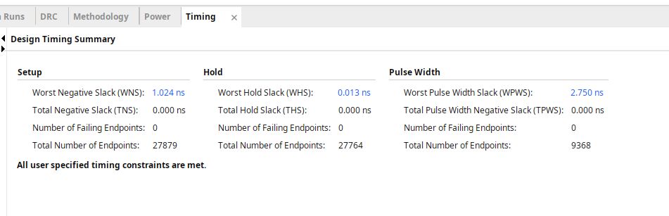
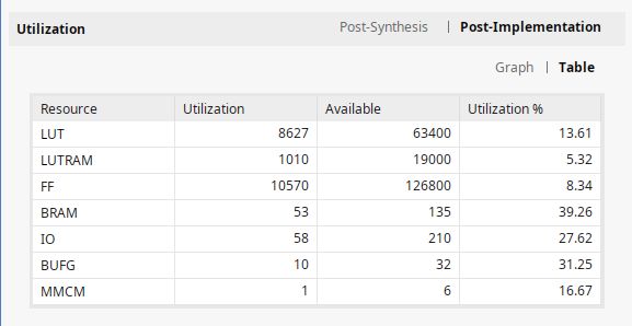
The captured implementation reports 1.024 ns of setup slack and no failing timing endpoints. Resource use includes 8,627 LUTs and 53 BRAM blocks. These figures describe the complete gateway, including processor and peripherals; they are not AES-only costs.
Fitting the board state into sixteen bytes
The ADT7420 temperature reading arrives over I²C. The SPI driver burst-reads six acceleration bytes from the ADXL362, reconstructing three signed values from the sensor’s little-endian register order. The packet builder then serializes the multibyte fields in big-endian order.
| Block bytes | Field | Representation |
|---|---|---|
0 | Sequence number | Unsigned byte, wraps after 255 |
1–2 | LED state | 16-bit mask |
3–4 | Switch state | 16-bit mask |
5 | Buttons | Lower five bits |
6–7 | Temperature | Raw ADT7420 register value |
8–9, 10–11, 12–13 | Acceleration X, Y, Z | Three signed 16-bit values |
14–15 | Reserved | Zero-filled |
Those sixteen bytes go through AES. A plaintext type byte, currently 0x01, is prepended afterwards. The receiver can identify the packet before decrypting it, and the UDP payload is exactly 17 bytes.
Writing the headers, then reading the screen
The firmware constructs a packed 42-byte header: 14 bytes of Ethernet, 20 of IPv4, and 8 of UDP. It fills in the addresses and lengths, calculates the IPv4 header checksum, and writes the header and encrypted payload to the Ethernet FIFO. Transmission uses broadcast addresses, so this small driver does not implement ARP.
On the computer, a listener thread checks packet length and type, decrypts with PyCryptodome, and puts the parsed state in a queue. The tkinter event loop drains that queue and displays the latest reading, keeping socket waits out of the UI thread. It converts the raw temperature to degrees Celsius and shows acceleration in mg, or thousandths of g.
Clicking LED 5 sends L5; LR and LL rotate the pattern. D1000 requests a one-second update interval, and K followed by 32 hexadecimal characters sets the key. There is also an accelerometer mode that moves the desktop window with the board.
A short, silent recording from the project: the board and the live controller side by side. This is the original demo, converted from GIF to a smaller video file.
Where the prototype stops
The gateway demonstrates the complete hardware-to-screen path, but encryption alone does not make its protocol ready for deployment. Blocks have no authentication or replay protection, and control commands—including key changes—are plain text. The receive driver also assumes a fixed header layout. Authenticated messages, key provisioning, and proper frame validation would be the next work before putting it on a shared network.
The repository contains the Vivado project, firmware, controller, testbenches, and original presentation. Start with the AES state machine, the AXI driver, or the packet builder, depending on which side of that path interests you.